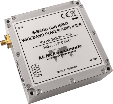
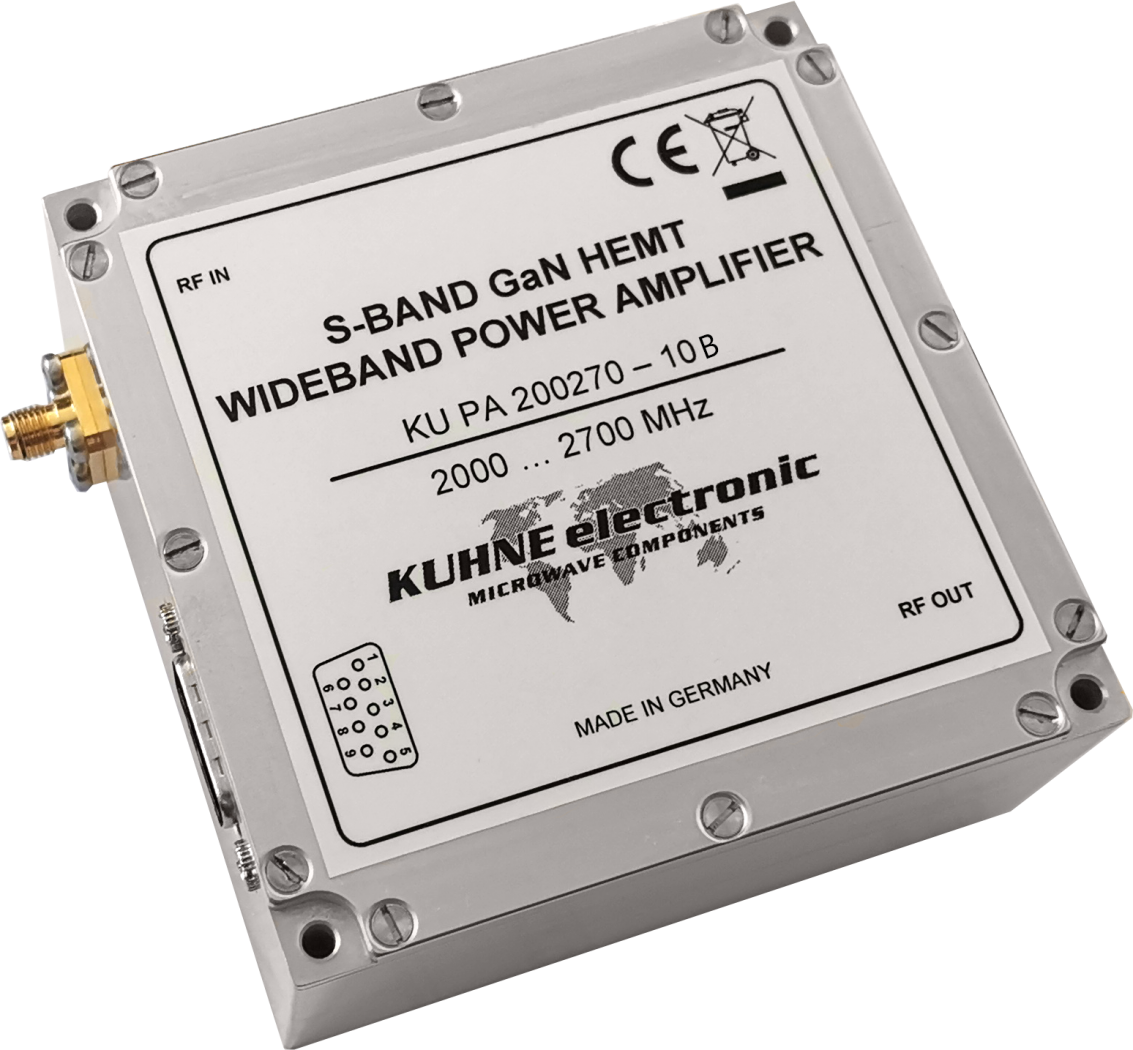
KU PA 200270-10 B, GaN-HEMT Power Amplifier
Based on GaN HEMT technology, the amplifier module achieves energy efficiencies greater than 40% over the entire 2000-2700MHz bandwidth at 10W output power.
Lead time on request
| Frequency range | 2000..2700 MHz |
| Maximum input power | +30 dBm |
| Output power P3dB | 40 dBm (min.) (CW) |
| 10 W (min.) (CW) | |
| Gain (small signal) | 47.5 dB (typ.) |
| Gain flatness (small signal) | +/-0.75 dB (typ.) |
| Noise figure @ 18 °C | 1.5 dB (typ.) |
| Harmonic rejection | 40 dB (typ.) |
| Over temperature protection | yes |
| IM3 (2) | 30 dBc (typ.) @ 40 dBm PEP |
| Efficiency | 40 % (typ.) @ P3dB |
| Input return loss (S11) | 13 dB (typ.) |
| ON voltage | +3 ... +50 V DC |
| Supply voltage | +10 ... 50 V DC |
| Quiescent current | 160mA (typ.) @ 28V DC |
| Current consumption | 3 A (max.) @ 10V DC |
| Forward detection | yes (log. detector) |
| Reflected power detection | yes (log. detector) |
| VSWR of load | infinite |
| Operating case temp. range | -20 ... +80 °C |
| Input connector / impedance | SMA-female / 50 ohms |
| Output connector / impedance | SMA-female / 50 ohms |
| Case | milled aluminium |
| Dimensions (mm) | 85 X 85 X 40 |
| Weight | 500 g (typ.) |
Based on GaN HEMT technology, the amplifier module achieves energy efficiencies greater than 40% over the entire 2000-2700MHz bandwidth at 10W output power. The amplifier is temperature compensated and, despite its high gain (47dB), features a very low gain ripple of typically +/- 0.5dB across the full bandwidth.
The high efficiency in combination with an extended operating temperature range of -20 ... + 80°C allows the use of the amplifier module even under suboptimal cooling conditions. An overtemperature shutdown at +80°C (with automatic restart) protects the module from overheating.
The RF output tolerates arbitrary mismatch without causing instability or damage.
In addition to the standard version with + 28V operating voltage (version A), the amplifier module is also available with wide-range supply voltage input (version B, +10 ... + 50V operating voltage).
The module provides low-impedance monitoring outputs for measurement and monitoring of forward and backward power as well as operating temperature. Power supply, control and monitoring signals are provided via a robust I/O interface (9-pin Sub-D connector) with protection against reverse polarity, overvoltage and EMI.
- High efficiency and bandwidth
- Very low ripple, noise figure and good harmonic rejection over the entire bandwidth
- Robust I/O interface via Sub-D connector with monitoring outputs for forward and backward power as well as temperature
- Extended operating temperature range -20 ... + 80 ° C
- Available with wide-range supply voltage input +10 ... 50V (version B)
- Plasma generation and microwave heating in process engineering and scientific applications
- RF Measurement setups, EMC testing
- Radar
- Jammer
- Analog & Digital Transmission Systems